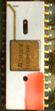
HP-35 Control &Timing chip.
|
|
HP-35 Control &Timing chip. |
The Control and Timing chip is probably the most complex circuit of the machine, handling all tasks related to the timing, so critical on a bit serial calculator.
- It contains the
micro-sequencer of the system and the master system counter,
- generates the ROM address and handles return address in case of subroutine
call,
- generates the synchronizing SYNC signal,
- generates the some WS signals (when the pointer P is involved),
- keeps status information for system and algorithms,
- and controls the keyboard scanning as part of the system counter.

|
|||||||||
| Vss | 1 | Control | 28 | WS | to A&R |
|
|||
| from clock driver | Ø1 | 2 | and | 27 | NC | ||||
| from clock driver | Ø2 | 3 | Timing | 26 | NC | ||||
| Gnd | 4 | circuit | 25 | SYNC | to ROM, to A&R | ||||
| from one shot | Init | 5 | 24 | NC | |||||
| to ROM | Ia | 6 | 1820-0849 | 23 | NC | ||||
| from A&R | Carry | 7 | 22 | KB Col 1 | |||||
| KB | Row 2 | 8 | 21 | KB Col 2 | |||||
| KB | Row 3 | 9 | 20 | KB Col 3 | |||||
| KB | Row 4 | 10 | 19 | KB Col 4 | |||||
| KB | Row 5 | 11 | 18 | KB Col 5 | |||||
| KB | Row 6 | 12 | 17 | Vgg | |||||
| KB | Row 7 | 13 | 16 | KB Row 1 | |||||
| KB | Row 8 | 14 | 15 | Is | from ROM | ||||
| fig 1 | |||||||||
1 - The micro-sequencer.
The control unit of the C&T -following the Wilkes' model- is micro-programmed: an operation can be broken down into a sequence of elementary operations named micro-operations, and grouped in a micro-program.
This is very similar –at a different level -to the program in the ROM of the calculator. In the programmable HP-65, for example, there are in fact 3 levels of programming –the micro-programmed sequencer, the firmware in ROM and the user’s program in RAM.
The micro-control unit consists of a decoding tree, two matrices and associated registers connected as indicated in Fig. 2. The decoding tree’s output lines pass through matrix A which outputs are the control lines operating the logic associated with micro-operations.
One input line of the matrix corresponds to one micro-order.
The output lines from the decoding tree also pass into a second matrix B, which outputs correspond to the address of the micro-order to be performed next in time. Gating alternately the address of micro-orders and the output of matrix B, causes a predetermined sequence of micro-orders to be executed.
In the general case, micro-program execution can be conditional using a conditional flip-flop (between the 2 matrices) ; in the HP-35’s C&T the carry flip/flop is set when the CARRY bit out of the adder in the arithmetic unit is set with WS also high.
The flip-flop is used to determining during the BRANCH “go to” instruction, if the current address should be incremented (Carry=1) or replaced by the “branch” address (Carry=0). Should the replacement occur, the control line BRH will gate the address on the Ia line.
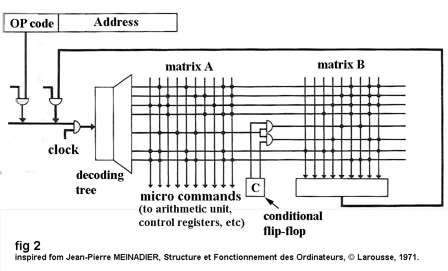
Note that control lines IST (if status bit is set) or IPT (if pointer <> n) is used in the same manner to implement the different flavours of branching instructions.
This micro-control unit comprises a 1450
bit ROM (58 words of 25 bits), receives inputs (qualifiers or status conditions)
from the entire system and emits control sequenced signals.
In the HP-35, the pulse used to clock sequencing is the phase 2 of the MOS clock
As indicated by Wilkes in his original paper, in a serial machine, the control signal must be critically timed. In fact, since most of the commands are issued only at certain part of the 56 bits word time, “timing” qualifying signals are checked: a simple example is the address increment during bit times b47-b54.
Pointer register state, 12 status bit states, PWO state are other conditions taken into account by the control unit (more on this below).
2- Program counter.
A 28 bit shift register which circulates twice each 56 bit word time, is employed to hold in three functional parts: the main ROM address register (eight bits), the subroutine return address register (eight bits) and the status register (12 bits).
The system read only memory is made of
768 (3 * 256) words (instructions) of 10 bits each, so addresses
are 8 bits wide (addresses are express in octal –relative to one of the 3 ROMs-
from 000 to 377.
The current address is circulating in C&T adder. It is incremented during the
time window b47-b54 to form the next instruction address and is gated to the Ia
line during time window b19-b26.
One important point is that this address
is transmitted to each of the 3 ROMs though only one is active at a time. The
“select rom x” instruction is used to set or reset a “Rom enable flip/flop”
(ROE) in each ROM (more on this in the relevant chapter).
The normal operation to form the next address is incrementing the current
address (program counter) but if during bit times b45-b46 a pattern “10” appears
signalling a “jsb” –jump to subroutine- instruction, the incremented current
address is saved and gated to the “return address” part of the 28 bit register,
and the remaining 8 bits are gated in the address part of the register,
preparing to jump to the subroutine during the next b19-b26 bit times.
At execution of the “return” instruction, the return address is inserted at the proper time in the 28 bits shift register commanded by the JSB control signal.
In case of a branch “go to” instruction,
only the substitution is made. The carry flip/flop is checked at bit time b19 to
take care eventually of the “conditional branching” (more on this later).
In the HP-35 architecture, the instruction set allows only one level of
subroutine; in the firmware, a current trick in the “state battle” was to re-use
a “jsb” instruction and to forget to “return”, jumping to another “jsb”.
Sometimes the code looks really de-structured.
Note also that –like at the game of Bridge- the programmer had to plan carefully communication between ROM; routines of the same class –Cordic for example- spanned across 2 ROMs space.
3 - Synchronizing the system and the system counter.
The system, as we have seen, is based on
a 56 bit serial word; it requires accurate synchronization.
A six (6) bit counter is used for counting up to 56.
Several timing signal are derived from this master counter:
The SYNC pulse is generated during bit times b45-b54 and transmitted to all
circuits particularly to each ROM that has its own 56 state counter,
synchronized to the system counter.
The pulse means that an “instruction” is on the Is bus and on the trailing edge other circuits are starting to count to 56,
The PWO line (power-on) has a main role
in the synchronization process particularly:
- it gets the address of micro-control ROM set to a proper starting state and,
- it synchronizes the master system counter with the counter in each ROM.
When the power is applied, a one shot
circuit (described later) holds the PWO line at logic 1 sufficiently to give
time to the C&T master system counter to count a few word time: the SYNC pulse
is high enough time to help synchronization.
After synchronization, ROM 0 is active, ROM 1 and ROM 2 are inactive and the
starting address “00000000” is in the address buffer ready to be gated on line
Ia.
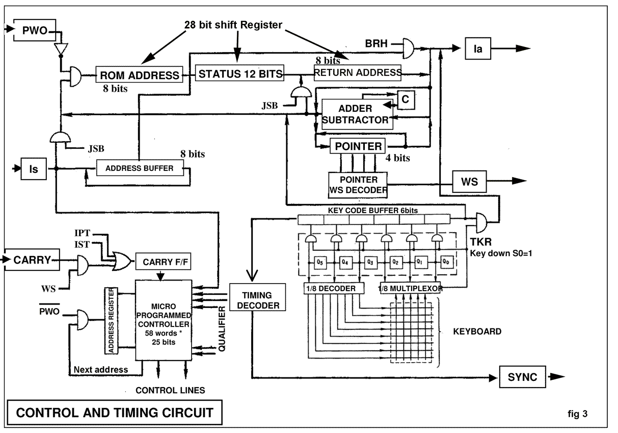
4 - The keyboard scanning.
The system master counter is also employed as a keyboard scanner. This could seem strange but deriving this function from the system counter and using a keyboard scanning technique directly interfaced to the MOS circuitry, reduces significantly circuit complexity.
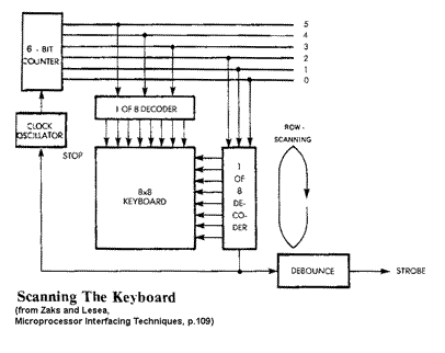 For
an insight of the sate of the art in the 70’s see “Microprocessor Interfacing
Techniques, Zaks and Lesea, Sybex p.100.
For
an insight of the sate of the art in the 70’s see “Microprocessor Interfacing
Techniques, Zaks and Lesea, Sybex p.100.
The most significant three bits of system counter –which change faster than the other ones- are decoded by a 1/8 decoder, which sequentially selects one of the keyboard row lines.
The least significant three bits of the system counter - count modulo seven and go to a 1/8 multiplexor, which sequentially selects one of the keyboard columns (during 16 clock times no key is scanned).
Every time a “1” is generated on a column, the 8 rows are scanned in turn.
Note that in this rather “raw” implementation there is no intrinsic “debouncing” feature: this will be handled by the firmware.
If a contact is detected at any intersection point in the five-by-eight matrix (by depressing a key), the key down signal will become high for one state of system counter and this state will be saved in key code buffer. This six-bit code is then transferred to the ROM address register and becomes a starting address for the routine executing the key function (the two missing leading 0 bits are added by hardware to have 8 bit address).
5 - The 12 status bits.
The status register (part of the 28 bit
register) contains 12 flags which are used to keep track of the state of the
system:
- S1, S2, S5, S9, S10 : switches between math functions,
- S3 : “CHS” key pressed,
- S4 : "EEX" key pressed,
- S5 context dependant,
- S6 "." has been pressed,
- S7 stack must be pushed,
- S8 key down not yet been processed,
- S10 “prefix” key “ARC”,
- S11 number entered with a mantissa.
etc.. (see the relevant chapter).
In each case the calculator remembers past events by setting the appropriate status bit.
Any status bit can be set, reset, or
interrogated while circulating through the adder in response to the appropriate
instruction. A positive answer to a status bit interrogation will set the carry
flip-flop as indicated by control signal IST.
Only one status bit is set and reset by the hardware: the status bit 0
indicating that a key has been pressed. In the HP-55 and HP-65, the “program
mode” selection will be signal by the hardware using a status bit.
6
- The pointer P and the WS signal.
a) Pointer P
The pointer p is a 4 bit register (from 0
to 13 decimal) that points to the requested digit of a 14 digit register. This
feature allows the A&R to operate on a portion of register (there are 2 options:
“pointer position” and “up to pointer position”).
This kind of feature makes the HP-35’s processor very specialized: set p to 12
allows exchanging all of a register except mantissa sign, for example.
There are instructions to set, increment, decrement, and interrogate pointer P.
The pointer is incremented or decremented
in the C&T address “adder/subtracter”.
If the answer to the instruction "is pointer #" is positive, the carry flip-flop
will be set (Carry=1) by the IPT signal.
b) WS when pointer P is involved
We will encounter the WS signal when studying the ROMs. It comes from the active ROM and signals to the A&R the in current instruction is to be executed only on a part of the designated register (mantissa, exponent, sign etc..).
The WS signals referring pointer P are
generated in the C&T:
- pointer only,
- up to pointer (pointer position and all less significant digits).
The C&T WS line is or-tied with the ROM word-select line and goes to the A&R.
A carry signal out of the adder in A&R, with WS high, will set carry flip-flop.
This flip-flop is interrogated during the BRANCH instruction to determine if the existing address should be incremented (carry=1) or replaced by the branch address (no carry). The branch address is retained in an eight-bit address buffer and gated to Ia line by the BRH signal.
Jacques Laporte,
18 January 2007.